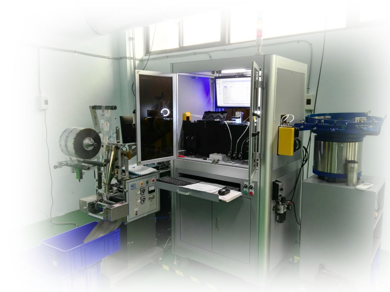
Optical Inspection System
System) is an automated tool that uses optical technology to inspect products or object surfaces. It is mainly used in industrial manufacturing processes to detect whether there are defects or abnormalities in products to ensure product quality. These systems are commonly used in high-precision industrial fields such as electronics, semiconductors, printed circuit boards (PCBs), and automotive parts.
Basic principles of optical detection systems
Optical inspection systems utilize optical devices (such as cameras, light sources, and lenses) to capture images of products or objects and analyze that image through image processing technology to detect potential defects or anomalies. Commonly used optical inspection technologies include:
2D inspection: Use a 2D camera to inspect flat images of objects and identify defects such as cracks, scratches, stains or abnormal shapes.
3D inspection: Obtain 3D images of objects through laser scanning or stereo vision technology to analyze their surface structure, shape or height differences.
Spectral analysis: Use different wavelengths of light to detect differences in different materials or components on the surface of an object.
Applications of optical detection systems
Semiconductor manufacturing: Detect subtle defects on the wafer surface to ensure high precision during the manufacturing process.
Printed circuit board (PCB) inspection: Detect solder joints, component mounting locations and connection problems on PCB.
automobile manufacturing: Inspect the dimensions and surface quality of automotive parts to ensure they meet design specifications.
Monitor production: Detect whether there are bright spots, dead spots, chromatic aberration and other problems on the display panel.
Medical device testing: Ensure medical products meet high standards of quality requirements.
Advantages of Optical Inspection Systems
High precision: Optical inspection technology can detect micron-level defects and anomalies, and is particularly suitable for manufacturing fields that require high precision.
Non-contact detection: Optical inspection does not require contact with the product surface, so it will not cause damage to the product.
Automated and high-speed inspection: Can realize fully automated detection, greatly improve production efficiency and reduce labor costs.
Adaptable: Different optical equipment and detection parameters can be flexibly configured according to different product types and detection needs.
Development trend
With advances in artificial intelligence (AI) and machine learning, optical inspection systems are constantly being upgraded. Through AI technology, these systems can automatically learn and optimize the detection process, reduce false detections and improve accuracy. In addition, with the advancement of Industry 4.0, optical inspection systems will be combined with more automated production equipment to achieve more intelligent factory operations.
Time spent testing equipment
definition
The time spent on inspection equipment refers to the total time required to complete an inspection task, which usually includes preparation time, inspection time and post-processing time. The length of this time directly affects the production efficiency of the equipment and the overall inspection process.
Image acquisition time:The time required from the start of shooting until the image is generated. For high-speed inspection systems, image acquisition times are usually very short.
Pre-processing time:After the image is acquired, it takes time to perform processing such as filtering, binarization, and denoising.
Feature extraction and analysis time:The time required for feature extraction, comparison and calculation of images to identify and detect specific targets.
Result output time:The time required to display or transmit the test results to the user interface, device system, etc.
Display mode
The time spent testing equipment is usually displayed numerically or graphically. Common display methods include:
Digital display:Displays the elapsed time as a specific time number (e.g. seconds, minutes).
Progress bar:Use a progress bar to display the ratio of elapsed time to total time during the detection process, allowing users to intuitively understand the progress.
Graphical reporting:Display the time spent on different detection tasks in the form of charts or graphs to facilitate analysis and comparison.
Display timing:
Instant display:Some devices can display the time taken for image processing in milliseconds in real time, allowing users to understand the operating status of the system.
Later statistical report:Some systems accumulate the average, maximum, and minimum times of all detection processes for performance analysis and optimization.
Delayed warning:On the production line, if the detection time exceeds the predetermined limit, the system will issue a delayed alarm for immediate processing.
time requirement
When designing testing equipment, time requirements should include the following aspects:
High-speed processing requirements:In industrial inspection or manufacturing processes, inspection equipment needs to be able to complete analysis in a very short time to avoid affecting the production rhythm. This typically requires a single detection to take anywhere from milliseconds to seconds.
Stability requirements:Not only is the equipment required to be fast, but it also needs to maintain consistent processing time in multiple inspections to avoid false detections or missed detections due to delay fluctuations.
Adjustability:Some applications may need to switch between different speeds, so the detection time needs to be flexible and adjustable to adapt to various application scenarios.
Results feedback requirements:For critical tasks, the detection results need to be fed back to the control system or user within a short period of time so that follow-up operations can be quickly carried out, such as fault shutdown or quality control adjustments.
Taken together, the time requirements and display of image detection equipment should be designed according to actual application requirements. For example, high-speed inspection on industrial lines requires low latency, while medical image processing may focus more on high accuracy and stability. If there are specific detection scenarios or requirements, the time control strategy can be further refined.
Detection time (Cycle Time)
definition
Detection time (Cycle Time) refers to the total time required from the beginning to the end of the detection task. This includes all related activities such as preparation, testing, data processing and results reporting. Testing time is an important indicator to evaluate the performance and production efficiency of testing equipment.
Calculation method
The calculation of detection time usually includes the following parts:
Preparation time:The time required to prepare for testing.
Detection time:The actual time required to perform the test.
Post-processing time:Including time for data analysis, results recording and report generation.
The total detection time can be expressed as:
Total detection time = preparation time + detection time + post-processing time
Influencing factors
Detection time can be affected by a variety of factors, including:
Equipment performance:The speed and accuracy of inspection equipment directly affect the inspection time.
Testing procedure:The complexity and number of detection steps affects the overall time.
Operator experience:Experienced operators can complete inspection tasks faster.
Environmental conditions:Factors such as ambient light and temperature may also affect the detection effect and thus the time.
How to optimize detection time
In order to improve detection efficiency, the following methods can be considered:
Standardized process:Develop standard operating procedures (SOP) to simplify testing steps.
Training operators:Improve operator skills and reduce delays caused by improper operation.
Equipment maintenance:Regularly maintain testing equipment to ensure it is operating at its best.
Data automation:Use automated tools to process data and reduce manual time.
in conclusion
Detection time (Cycle Time) is an important indicator for evaluating detection efficiency. Understanding its definition and influencing factors can help optimize the detection process and improve overall production efficiency.
Filter noise problem in image detection
Noise is unwanted noise or outliers in an image, which can result from sensor failure, lighting changes, or other external factors. These noise points will affect the accuracy of image detection.
During the image detection process, there are usually some noise interferences, which may affect the final detection results. In order to eliminate noise, the following methods can help improve image quality:
Binarization threshold
Thresholding:Set a threshold and label pixels above or below this value as noise and then process them. Convert the image to black and white and use threshold settings to remove noise smaller than the threshold, but some details may be lost.
Common ones include global binarization, local binarization or adaptive binarization.
filter
Image smoothing:Use a smoothing filter, such as a Gaussian filter, to reduce the effects of noise.
Mean filter:Averaging pixels in an image smoothes noise but can also blur detail.
Median filter:Replace each pixel in the image with the median of surrounding pixels to remove isolated noise.
Frequency domain processing
Use Fourier Transform to convert the image into the frequency domain, remove high-frequency noise and retain low-frequency components, which is suitable for processing periodic or random noise.
Frequency domain filtering/Gaussian filtering:Convert the image to the frequency domain and use a low-pass filter to remove high-frequency noise. Gaussian function is used for smoothing, which is suitable for removing high-frequency noise.
Morphological operations
Expansion and erosion:Use etch and dilation operations to remove small spots or fill small holes, and correct image edges.
Opening and closing operations:The opening operation (erosion followed by dilation) is used to remove small objects, and the closing operation (dilation followed by erosion) is used to fill small holes.
Convolutional Neural Network (CNN)
Use the trained deep learning model for image denoising, which is especially suitable for high-resolution images or images with a wide variety of noise points.
These methods can be used alone or in combination, depending on the characteristics of the image and the detection needs.
Tools and techniques for filtering
The following tools and techniques can be used to filter image noise:
OpenCV: A powerful computer vision library that provides a variety of filtering and image processing functions.
PIL (Python Imaging Library): can be used for basic image processing and noise filtering.
MATLAB: Provides a powerful image processing toolbox for advanced image analysis.
in conclusion
Filtering noise is a key step in image inspection. Choosing the appropriate filtering method can significantly improve detection accuracy, thereby improving overall system performance.
Optical inspection dimensional measurement
1. Non-contact measurement
Optical inspection technology is a non-contact measurement method that uses optical sensors, cameras or lasers to obtain dimensional data of the measured object. Such technology is very suitable for high-precision and hard-to-touch objects, avoiding deformation or damage caused by contact, and is suitable for the measurement of tiny components or fragile materials.
Laser Range Finder: Use the time difference of laser reflection to accurately measure the distance or size of an object.
triangulation: Laser or beam is projected on the object, and the position of the reflection point is captured by a camera or photoelectric sensor to calculate the size.
2. 3D image processing
Optical inspection technology can generate 3D images and perform dimensional measurements. Through multi-view image fusion or stereo vision technology, the software can quickly generate accurate 3D models to measure height, depth and other geometric features.
Stereo Vision: Use two cameras to shoot objects from different angles, obtain depth information by calculating the displacement between the two images, and then calculate the three-dimensional size of the object.
Structured light projection: Project striped light patterns onto the surface of objects, and reconstruct the 3D shape and size of the object based on the deformed light strips.
3. Precision detection and error control
Optical inspection technology can perform dimensional measurements with micron or even higher precision and is often used for product quality control in industrial production. It can effectively detect whether the workpiece meets dimensional tolerances and can instantly detect errors during processing.
Optical Measuring Machine: Combined with high-resolution optical components and software algorithms, it can quickly perform multi-point measurements and is suitable for complex-shaped objects.
Interferometry: Based on the interference phenomenon of light waves, it can measure surface shape and size with nanometer-level accuracy.
4. Rapid processing and instant detection
When using optical detection technology for dimensional measurement, combined with automated software and image processing algorithms, real-time measurement and data analysis can be achieved, reducing manual intervention.
Automated image inspection system (AOI): This type of system combines machine vision and image processing technology to instantly detect whether the size of the product meets specifications on the production line.
5. Flexible application scenarios
The flexibility of optical inspection tools allows them to be used effectively in different scenarios. By selecting different optical measurement tools, the measurement methods and tools can be adjusted according to the material, shape, size and other requirements of the measurement object.
in conclusion
Optical inspection technology has the advantages of non-contact, high precision, speed and flexibility in dimensional measurement. In particular, 3D image processing applications can greatly speed up inspection development. It has become an indispensable and important technical tool in industrial automation, quality control and precision manufacturing.
Screw size
definition
Screw size refers to the diameter, pitch, length and other geometric characteristics of the screw, which are used to indicate the specifications and applicable scope of the screw. Different sizes determine the strength of the screw, the diameter of the mating part and its use.
Common expressions
Screw size is usually expressed as "diameter × pitch × length", for example:
M6 × 1.0 × 20 → Indicates metric screws, diameter 6 mm, pitch 1.0 mm, length 20 mm.
1/4"-20 × 1" → Indicates inch screws, diameter 1/4 inch, thread number 20/inch, length 1 inch.
Main size items
Thread outer diameter (Major Diameter): The maximum diameter between screw peaks.
Pitch: The axial distance between adjacent tooth crests.
Length: The distance from the bottom of the nut or the bottom surface of the head to the end of the thread.
Head Size: Depends on the screw head type, such as hexagonal head, cross head, inner hexagonal head, etc.
Common specifications of metric screws (ISO)
Thread specifications
Outer diameter (mm)
Standard pitch (mm)
Common length (mm)
M3
3.0
0.5
6~40
M4
4.0
0.7
8~50
M5
5.0
0.8
10~60
M6
6.0
1.0
10~80
M8
8.0
1.25
15~100
M10
10.0
1.5
20~120
M12
12.0
1.75
25~150
Common specifications of inch screws (UNC/UNF)
Thread specifications
Outside diameter (inch)
Number of teeth (per inch)
Common length (inch)
#6-32 UNC
0.138
32
1/4"~2"
#8-32 UNC
0.164
32
1/4"~2"
1/4"-20 UNC
0.250
20
1/2"~3"
5/16"-18 UNC
0.313
18
1/2"~3"
3/8"-16 UNC
0.375
16
3/4"~4"
Application scope
M3~M6: electronic equipment, small machinery, home appliances.
M8~M12: automobiles and motorcycles, mechanical equipment, structural parts.
British UNC series: American equipment and imported industrial products.
Things to note
The size must be selected to match the pore size and material strength.
Do not mix threads with different pitches, otherwise the threads will be damaged.
It is necessary to consider whether the length of the screw penetrates or affects the structural strength.
Measuring key dimensions of screws
definition
Screw critical dimension measurement is the process of accurately detecting the main geometric features that affect screw performance, fit and strength. These dimensions are directly related to the assembly quality and safety of screws and nuts, hole positions or components.
Main measurement items
The key dimensions of screws can be divided into two categories: thread part and head:
Thread size:
Major Diameter: The maximum diameter between the thread peaks determines the fit between the screw and the hole.
Minor Diameter: The minimum diameter at the bottom of the screw thread, which affects the strength of the screw.
Pitch Diameter: The imaginary diameter where the thread thickness intersects with the pitch line is a key parameter for judging the thread fit accuracy.
Pitch: The axial distance between adjacent tooth crests affects the screw-in speed and fit.
Thread Angle: Generally, the metric thread is 60°, and the inch thread also mostly adopts this angle.
Head size:
Head Diameter: Determine the force-bearing area and tool coordination.
Head Height: Affects torque application and structural appearance.
Across Flats (AF): Corresponding size of hexagonal screw wrench or socket.
Hex Socket Size: Corresponds to hexagon socket wrench specifications.
Common measurement tools
Vernier Caliper: Measuring outer diameter, inner diameter, head size, etc.
Thread Ring Gauge and Thread Plug Gauge: Check whether the outer diameter and pitch of the thread meet the specifications.
Threaded Projector (Optical Comparator): Magnify the tooth shape angle and tooth profile.
Three coordinate measuring machine (CMM): High-precision measurement of pitch diameter and geometric tolerance.
Inch system: 2A (external thread), 2B (internal thread)
Quality inspection focus
Errors in outer diameter and middle diameter will lead to uneven fit.
Tooth pitch or tooth angle errors will affect the smoothness of screwing in.
Deviation in head size may cause poor torque application.
Measuring tools need to be calibrated regularly to ensure measurement accuracy.
Application scope
Screw size measurement is widely used in:
Precision machinery manufacturing and quality control
Automobile and motorcycle parts inspection
Aerospace and electronic component assembly inspection
Thread mold and gauge manufacturing
Geometric tolerance
definition
Geometric Tolerance is a technical standard used to control the accuracy of part geometry, direction, position and runout. It ensures that parts can meet the design functional requirements during the manufacturing and assembly process, and that even if there are minor errors, they can still operate correctly and cooperate with each other.
Classification
Geometric tolerances can be divided into four major categories according to control items:
Form Tolerance: Controls the shape accuracy of a single feature, for example:
Straightness
Flatness
Roundness
Cylindricity
Orientation Tolerance: Controls the angle or direction between features, for example:
Parallelism
Perpendicularity
Angularity
Location Tolerance: Controls the accuracy of the relative position of features, for example:
Concentricity
Symmetry
Position
Runout Tolerance: Controls the radial or axial change of the rotated feature, for example:
Circular Runout
Total Runout
symbolic representation
Each geometric tolerance is represented on technical drawings by an international standard symbol (such as ISO 1101 or ASME Y14.5), for example:
⏤ Flatness
○ Roundness
⌓ Cylindricity
∥ Parallelism
⊥ Verticality
⌖ Location
tolerance grid
In engineering drawings, geometric tolerances are marked with "Feature Control Frame", which includes:
Geometric tolerance symbols
Tolerance value
Datum symbol (if required)
For example:⊥ 0.02 AIndicates that the verticality error of this feature relative to datum A shall not exceed 0.02 mm.
Application purpose
Ensure parts interchangeability and assembly accuracy
Reduce unnecessary processing accuracy requirements and reduce costs
Clearly define functional areas and critical dimensions
Improve quality inspection and communication consistency
Use Python to calculate roundness, concentricity and surface roughness
1. Roundness
True roundness can be calculated using the least squares circle method, where the deviation from the theoretical circle is calculated for a set of points.
Concentricity determines the deviation by calculating the distance between the centers of the inner and outer rings.
# Assume the center coordinates of the inner and outer circles
inner_center = (ix, iy)
outer_center = (ox, oy)

def calc_concentricity(inner_center, outer_center):
    return np.sqrt((inner_center[0] - outer_center[0]) ** 2 + (inner_center[1] - outer_center[1]) ** 2)

concentricity = calc_concentricity(inner_center, outer_center)
print("Concentricity deviation:", concentricity)
3. Surface Roughness
Surface roughness can be calculated from the Ra value, which represents the mean absolute deviation of a measurement point from a mean line.
def calc_surface_roughness(profile_points):
    mean_line = np.mean(profile_points)
    ra = np.mean(np.abs(profile_points - mean_line))
    return ra

# profile_points represents surface roughness measurement points
profile_points = np.array([...])
roughness = calc_surface_roughness(profile_points)
print("Surface roughness Ra value:", roughness)
Cylindricity
definition
Cylindricity is a type of geometric tolerance that is used to evaluate the deviation of the surface or axis of an object from an ideal cylinder in three-dimensional space. It describes the geometric error of the actual surface relative to the ideal cylindrical surface, ensuring that the parts have the correct shape and fit accuracy.
Measurement method
The detection of cylindricity is usually carried out using a three-dimensional coordinate measuring machine (CMM) or a special roundness meter. An ideal cylinder model is established through multi-point sampling, and then the maximum and minimum deviations from the actual surface to the ideal cylinder are calculated. The difference between the two is the cylindricity error.
Symbols and Tolerance Markings
In technical drawings, the tolerance symbol for cylindricity is "⌓". The marking method is as follows: Example: ⌓ 0.01, which means that the actual surface needs to be between two coaxial cylindrical surfaces with a radius difference of 0.01 mm.
application
Cylindricity is widely used in parts such as shafts, holes, and bearing seats that require high-precision fit. Controlling cylindricity avoids:
Poor fit between shaft and hole
Unstable operation or increased wear and tear
Seal failure
Differences from other tolerances
Cylindricity only controls shape error and does not involve position or orientation errors;
"Coaxiality" and "roundness" respectively control the error of axis position and cross-section circularity. The cylindricity range encompasses the overall three-dimensional shape and is more tightly controlled than roundness.
Various practical optical inspections
Workpiece color color deviation sorting and screening machine
Machine introduction
The workpiece color deviation sorting and screening machine is a high-precision screening equipment specially designed to distinguish subtle color differences. This equipment can effectively screen workpieces with very similar colors to ensure color consistency during the production process, and is suitable for industries that require strict color control.
Working principle
This screening machine is equipped with sophisticated optical sensors and an advanced color shift recognition system. As workpieces pass through the conveyor belt, the equipment detects subtle differences in color and sorts the workpieces into corresponding color areas based on set criteria.
Main functions
Micro color shift detection: Able to identify very close colors for fine classification.
Automated grading: Automatically classify according to color deviations to reduce manual errors.
Real-time data analysis: Real-time monitoring of the color data of each workpiece and continuous adjustment of screening criteria.
Application scenarios
This screening machine is widely used in industries with extremely high color requirements, such as precision manufacturing, automotive spray painting, and electronic component assembly. It can effectively distinguish workpieces of different shades or color deviations in the same color system, improving product consistency and quality.
advantage
Accurate color screening to reduce color deviation.
Improve production efficiency and adapt to the needs of efficient mass production.
Easy to operate and save labor costs.
Optical inspection of electronic components
What is optical inspection of electronic components?
Optical Inspection for Electronic Components
Components) is an inspection method that uses optical technology to inspect the appearance and quality of electronic components. Through high-resolution cameras and advanced image processing technology, optical inspection can identify defects, damage or deviations on component surfaces, and automate the inspection process to improve inspection accuracy and efficiency.
How optical detection works
The working principle of optical inspection of electronic components is as follows:
Use a high-resolution camera to scan the surface of electronic components and capture high-quality images.
Image analysis is performed through image processing software to check the appearance, size, shape and other characteristics of the component.
Automatically identify defects such as poor solder joints, component offsets, cracks or dirt, and record the inspection results.
Screen abnormal or defective components from the production line for further inspection or repair.
Optical detection applications
Circuit board manufacturing:Inspect solder joints, soldering quality and component positioning during printed circuit board (PCB) production.
Semiconductor testing:Inspect chip packages for defects such as scratches, dirt or oxidation.
Consumer electronics:Check the appearance quality of various consumer electronic components, such as resistors, capacitors, and IC components to ensure product consistency.
Advantages and Disadvantages of Optical Inspection
advantage:Non-contact detection, fast speed, high accuracy, and the ability to automate a large number of inspections.
shortcoming:It may be difficult to accurately detect transparent or reflective materials, and the equipment investment cost is high.
in conclusion
Optical inspection of electronic components plays a key role in the electronics manufacturing industry. Through fast and accurate inspection methods, it can effectively improve product quality and reduce defect rates, which is of great significance in ensuring the reliability and performance of electronic equipment.
Passive component appearance inspection machine
What is a passive component visual inspection machine?
Passive component appearance inspection machine is an automated equipment specially designed to inspect the appearance quality of passive components. Passive components such as resistors, capacitors and inductors must ensure that their appearance is flawless in order to work properly in electronic products. The appearance inspection machine can quickly and accurately detect whether the appearance of components meets quality requirements.
Core functions of appearance inspection machine
The main functions of the visual inspection machine include:
Defect detection:Detect whether there are defects such as scratches, cracks, contamination or deformation on the component surface.
Dimensions:Accurately measure component dimensions to ensure compliance with design specifications and avoid installation or performance issues.
Color detection:Check whether the component colors and markings are correct to identify components of different specifications.
Coding identification:Check the printed code on the component through image recognition to ensure correct identification.
Common detection techniques
Passive component visual inspection machines use a variety of technologies to perform inspection:
Image processing technology:A high-resolution camera is used to capture the appearance of the component, and image processing software is used to detect defects and measure dimensions.
Optical inspection:Optical sensors are used to inspect the appearance characteristics of components and detect minor flaws or dimensional deviations.
AI model:Combined with machine learning models, a large amount of detection data is analyzed to improve detection accuracy and efficiency.
Application examples
Passive component visual inspection machines are widely used in the electronics manufacturing industry. For example, in capacitor production lines, inspection machines can instantly screen out products with poor appearance to ensure that the quality of components entering the assembly process is correct, thereby improving the reliability of the final product.
Diode appearance inspection machine
What is a diode visual inspection machine?
The diode appearance inspection machine is an automated inspection equipment specially used to detect the appearance quality of diodes. Since diodes play an important role in circuits, it is important to ensure that their appearance is flawless to prevent product failure. The appearance inspection machine can efficiently and accurately screen out diodes with poor appearance and improve the product quality of the production line.
Core functions of diode appearance inspection machine
The main functions of the diode appearance inspection machine include:
Defect detection:Inspect the diode surface for scratches, cracks, contamination or other defects.
Size detection:Measure the length, width, and height of the diode to ensure it meets manufacturing specifications.
Electrode position detection:Confirm that the diode's electrodes are intact and properly aligned to ensure installation accuracy.
Coding and identification checks:Identify the markings and codes on the surface of the diode to identify different types and specifications of diodes.
Common detection techniques
Diode visual inspection machines typically use the following techniques for inspection:
Image processing technology:A high-resolution camera is used to photograph the diode surface, and image processing software is used to detect defects and measure dimensions.
Optical inspection:Use optical sensors to check surface defects and dimensional deviations of diodes to ensure that the appearance quality is up to standard.
AI-driven defect detection:Identifying defects through machine learning models can improve detection accuracy and adapt to different types of diode detection needs.
Application examples
Diode appearance inspection machines are widely used in the field of electronic component manufacturing. For example, on the diode production line, the inspection machine can instantly screen out products with poor appearance, ensuring that high-quality diodes are supplied to downstream assembly processes, further improving the reliability and stability of electronic products.
Optical inspection equipment is an important tool for inspecting the appearance and structural integrity of electrolytic capacitors. These devices can quickly and accurately detect appearance defects of capacitors through high-precision cameras and image processing technology. The following is an introduction to common electrolytic capacitor optical detection equipment:
1. Automatic optical inspection equipment (AOI)
Automatic optical inspection equipment (AOI) is mainly used for visual inspection of electrolytic capacitors. Through high-resolution cameras and image processing systems, AOI can detect the following defects:
Cracks or scratches on the surface of the capacitor
Poorly printed marks or labels
Electrode deformed or damaged
Packaging defects
2. X-ray inspection equipment
X-ray inspection equipment can detect the internal structure of electrolytic capacitors to ensure that there are no hidden flaws inside. This device can detect the following problems:
Broken internal wires or contacts
Electrolyte leakage or residue
Internal short circuit between layers
3. Laser measurement equipment
Laser measuring equipment can be used to measure the size and shape of electrolytic capacitors. Through laser scanning technology, it is possible to accurately detect whether the appearance and dimensions of the product meet the standards.
4. High-speed camera detection system
The high-speed camera system can perform real-time detection and is suitable for quickly detecting the appearance quality of electrolytic capacitors on the production line, and promptly detecting and eliminating defective products.
in conclusion
Electrolytic capacitor optical inspection equipment can help improve production efficiency and ensure product quality through advanced image processing and inspection technology, especially playing a key role in mass production.
PCB optical inspection
What is PCB optical inspection?
PCB optical inspection (Printed Circuit Board Optical
Inspection) is a technology that uses optical equipment to inspect printed circuit boards. Its main purpose is to check the manufacturing quality of the PCB, including the integrity of the solder joints, the correctness of the components and the connectivity of the circuits.
Types of PCB optical inspection
Common types of PCB optical inspection include:
Automated Optical Inspection (AOI):Use a high-resolution camera to scan the PCB to detect defects such as short circuits, open circuits and incorrect component locations.
X-ray inspection (AXI):Used to check internal structures, such as the solder joint quality of multi-layer PCBs.
Laser scanning detection:Use laser technology to detect surface height changes to ensure welding uniformity.
PCB optical inspection process
The optical inspection process usually includes the following steps:
Image capture:Use an optical camera to obtain high-resolution images of the PCB.
Image processing:The software analyzes the image to detect abnormalities such as welding defects or circuit interruptions.
Data comparison:Compare inspection results to design specifications to identify possible defects.
Advantages of PCB optical inspection
Optical inspection offers the following advantages:
High precision:It can detect tiny defects and is suitable for quality control of precision PCBs.
Contactless:It avoids any damage to the PCB and is suitable for the detection of high-value products.
High efficiency:Automated inspection greatly increases inspection speed and reduces labor costs.
PCB optical inspection challenges
Although optical detection technology is mature, it still faces some challenges:
Detection complexity:As the complexity of PCB design increases, inspection software needs to have higher recognition capabilities.
Equipment cost:High-resolution cameras and optical systems are more expensive.
False positive problem:Inspection software may identify normal variations as defects, increasing rework costs.
future development direction
With the introduction of AI and deep learning technology, PCB optical inspection is developing in an intelligent direction. These technologies will improve the accuracy of defect detection and further reduce false positives. At the same time, combined with automated production lines, optical inspection will become an efficient and reliable means of quality assurance.
Gold finger scratch detection
What is gold finger scratch detection?
Gold finger scratch detection is a surface defect detection technology that focuses on the gold finger part of the printed circuit board (PCB). The gold finger is the electrical contact part on the PCB and is responsible for signal transmission with the connector. Any scratches may affect its conductive performance and reliability.
The Importance of Gold Finger Scratch Detection
Reasons for gold finger scratch testing include:
Ensure electrical conductivity:Avoid scratches resulting in poor signal transmission or poor contact.
Improve product life:Protect gold fingers from physical damage and extend the life of PCB.
Quality assurance:Ensure PCB meets industry standards and meets customer needs.
Gold finger scratch detection technology
Commonly used gold finger scratch detection technologies include:
Optical Inspection (AOI):Use high-resolution cameras to detect surface scratches, stains and other defects.
Laser scanning:Use laser scanning technology to detect tiny unevenness or scratches on the surface of the gold finger.
Resistance test:Measure the resistance change of the gold finger contact point to determine whether there is damage.
Microscopic observation:Use an electron microscope to magnify the gold finger and detect minor scratches.
Gold finger scratch detection process
Typical testing procedures include:
Preparation stage:Place the PCB on the detection equipment and calibrate the detection position of the gold finger.
Detection stage:Scan the gold finger surface using selected detection technology and record any anomalies.
Result analysis:Analyze inspection data and classify qualified products and non-conforming products.
Report generation:Generate an inspection report detailing the location and severity of scratches.
Challenges of gold finger scratch detection
The detection process may face the following challenges:
High detection accuracy requirements:The scratches on the gold finger surface are usually very small, which requires high resolution of the detection equipment.
Reflected light interference:The gold finger material is highly reflective and may interfere with the accuracy of optical detection.
High-speed detection requirements:Rapid detection is required in a mass production environment, which poses challenges to equipment performance.
future development direction
In the future, Golden Finger scratch detection will combine artificial intelligence and big data analysis technology to achieve more efficient and intelligent defect detection. At the same time, optical and laser technologies are improved to overcome the problem of reflected light interference and further improve detection accuracy.
Lead frame optical inspection
What is leadframe optical inspection?
Lead frame optical inspection is a technical method that uses optical technology to inspect defects or defects that may occur during the manufacturing process of lead frames. Lead frame is an important part of semiconductor components, and its quality directly affects the performance and reliability of the overall product.
The Importance of Optical Inspection of Lead Frames
Optical inspection can ensure the following quality requirements of the lead frame:
Precision:Check whether the dimensions of the lead frame comply with the design specifications.
Surface integrity:Check for scratches, cracks or contamination.
Contact performance:Make sure the lead frame contact points are flawless to ensure conductive performance.
Lead frame optical inspection technology
Commonly used techniques in optical inspection include:
Automated Optical Inspection (AOI):Rapidly detect defects using high-resolution cameras and image processing technology.
Laser scanning technology:Detect small deformations or cracks on the surface of the lead frame.
3D optical measurement:Accurately measure the three-dimensional structure and size of the lead frame.
Microscopic optical inspection:Examine small surface imperfections with high-magnification microscopy.
Lead frame optical inspection process
The typical detection process is as follows:
Equipment preparation:Place the lead frame in the testing equipment to ensure accurate positioning.
Image capture:High-resolution images of the lead frame are captured through the optical system.
Defect analysis:Use image processing algorithms to analyze the type and location of defects.
Classification results:According to the test results, the lead frame is divided into qualified products and defective products.
Advantages of Leadframe Optical Inspection
Optical inspection offers the following advantages:
High precision:Able to detect micron-level defects.
Contactless:The inspection process will not cause any damage to the lead frame.
automation:A large number of lead frames can be processed quickly, making it suitable for large-scale production environments.
Data record:The inspection process can generate detailed inspection reports to facilitate traceability and improvement.
Challenges of Leadframe Optical Inspection
Lead frame optical inspection may face the following challenges:
High precision requirements:The structure of the lead frame is very small and requires high-resolution inspection equipment.
Diversification flaws:Different types of defects such as scratches, contamination, and deformation require different detection algorithms.
Detection speed:In mass production, it is necessary to maintain high speed while ensuring high precision.
future development direction
In the future, lead frame optical inspection will combine artificial intelligence technology to optimize defect classification and detection algorithms, and further improve detection speed and accuracy. At the same time, more comprehensive structural analysis will be achieved by introducing more advanced 3D imaging technologies. In addition, portable and modular testing equipment will facilitate rapid on-site testing.
Optical inspection of connector terminals
What is connector terminal optical inspection?
Optical inspection of connector terminals is an inspection method that uses optical technology to detect the size, shape and surface quality of connector terminals. This technology can effectively detect defects during the manufacturing process, such as deformation, scratches, contamination, or dimensional discrepancies, thereby ensuring product reliability and performance.
The Importance of Optical Inspection of Connector Terminals
Optical inspection has the following importance in connector terminal manufacturing:
Ensure connection reliability:Check that the contact points are flat and flawless to ensure a good electrical connection.
Improve product quality:Prevent defective products from flowing into the market and enhance user trust.
Reduce maintenance costs:Early detection of problems helps reduce subsequent repair and return costs.
Connector terminal optical inspection technology
The following are commonly used optical inspection techniques:
Automated Optical Inspection (AOI):Automatic inspection of terminal surfaces and structures using high-speed cameras.
3D optical inspection:Three-dimensional imaging technology is used to analyze the shape and height differences of terminals.
Micro-optical technology:Zoom in to inspect the terminal for fine structures and imperfections.
Laser scanning technology:Quickly scan terminal surfaces to detect deformation and dimensional deviations.
Connector terminal optical inspection process
The typical detection process is as follows:
Preparation stage:Secure the connector terminals in the testing equipment to ensure a stable position.
Image capture:Obtain image data of the terminal through a high-resolution camera or microscope.
Data analysis:Use image processing algorithms for defect identification and classification.
Result output:Generate inspection reports and mark defective products.
Advantages of Optical Inspection of Connector Terminals
This detection method has the following advantages:
High precision:Capable of detecting micron-level dimensional deviations and surface defects.
Contactless:Avoid physical damage to the terminals.
Fast and efficient:Suitable for testing needs of mass production.
automation:Reduce human factor interference and improve detection accuracy.
Challenges of Optical Inspection of Connector Terminals
The following challenges may be faced during optical inspection:
Complex structure:Some terminals are precision designed and require higher equipment resolution for detection.
Surface reflective:Reflection from metal terminals may affect the accuracy of image capture.
Environmental interference:External light or vibration may affect the test results.
future development direction
With the development of artificial intelligence and deep learning technology, optical inspection will become more intelligent. Future detection systems will be able to automatically learn and improve detection algorithms to further improve detection efficiency and accuracy. In addition, the combination of portable testing equipment and real-time data analysis technology will help achieve more flexible production monitoring and quality control.
Photoelectric component detection
Definition of optoelectronic components
Optoelectronic components are a type of electronic components that can convert light energy into electrical energy, or use electrical energy to generate light. Such components are widely used in optical communications, display technology, photovoltaic power generation and other fields. Common optoelectronic components include photoresistors, photodiodes, phototransistors and LEDs.
The purpose of photoelectric component testing
The main purpose of photoelectric component testing is to ensure stable component performance, good response speed, and reliability during its service life. Testing items usually include sensitivity, response speed, power conversion efficiency and environmental tolerance.
Core technology of detection
Optoelectronic component inspection usually uses the following core technologies:
Spectrum test:Measure the response ability of the component at different wavelengths to determine its spectral sensitivity.
Photoelectric conversion efficiency test:Detects the efficiency with which an element converts light into electricity, such as that of a photovoltaic cell.
Time response test:Test the response speed of the component to ensure it can still work accurately in rapidly changing light environments.
Stability and durability testing:Test under extreme temperature, humidity and other conditions to evaluate the long-term reliability of components.
Application examples
Optoelectronic component detection is widely used in industrial, medical and consumer electronics fields. For example, solar panels need to regularly check the conversion efficiency to ensure power generation efficiency; optical sensors need to respond quickly to detection in self-driving cars to ensure driving safety.
Solar panel optical inspection
What is solar panel optical inspection?
Solar panel optical inspection is a method that uses optical technology to detect defects or anomalies that may occur during the solar panel manufacturing process. This technology helps ensure the quality, efficiency and longevity of solar panels.
The purpose of solar panel optical inspection
The main purposes of optical inspection are:
Identify manufacturing defects:Detect cracks, chips or other structural problems.
Ensure performance consistency:Check the consistency between cells to ensure output efficiency.
Reduce losses:Detect problems early and fix them to reduce production losses.
Solar panel optical inspection technology
Common detection techniques include:
EL detection:Detect internal cracks and microcracks using electroluminescence technology.
PL detection:Photoluminescence technology is used to analyze the uniformity of the material's internal structure.
Infrared thermal imaging:Detect hot spots and poor welding problems.
High-resolution optical photography:Quickly capture surface defects such as scratches or contamination.
Solar panel optical inspection process
The standard testing process includes:
Light source selection:Select an appropriate light source, such as infrared light or ultraviolet light, according to the detection needs.
Image capture:Use a high-resolution camera or sensor to capture images of solar panels.
Image analysis:Use professional image processing software for defect identification and classification.
Report generation:Generate a detection report to record the location and nature of the problem.
Advantages of Solar Panel Optical Inspection
This technology has the following advantages:
Contactless:Will not cause any damage to solar panels.
High precision:Able to detect tiny cracks and defects.
High efficiency:Suitable for rapid detection needs in mass production.
Wide applicability:Suitable for various materials and types of solar panels.
Challenges of Solar Panel Optical Inspection
The detection process may face the following challenges:
High equipment costs:High-precision optical inspection equipment is expensive.
Data processing is complex:The large amount of data generated during the inspection process needs to be processed efficiently.
Environmental interference:External light sources or reflections may affect detection results.
future development direction
With the advancement of artificial intelligence and automation technology, future solar panel optical inspection will be more intelligent and efficient. Combined with deep learning algorithms, defects can be more accurately identified and classified, and inspection costs can be further reduced. In addition, the development of portable testing equipment will make on-site testing more flexible and convenient.
Tool drill bit inspection
The necessity of tool drill bit inspection
Tool drills are important tools in mechanical processing, and their status directly affects processing quality and production efficiency. Regularly testing the wear, accuracy and other performance parameters of cutting tools and drill bits can help maintain stable processing quality, extend tool life, and reduce production costs.
Core items of testing
The main items of tool drill bit inspection include:
Wear detection:Detect the wear of tool edges and drill tips to ensure cutting efficiency and reduce machined surface defects.
Accuracy testing:Ensure that the geometry and size of cutting tools and drill bits meet design requirements to ensure processing accuracy.
Surface roughness detection:Measure the surface roughness of cutting tools and drill bits to avoid excessive wear and affect the quality of processed surfaces.
Hardness test:Check the hardness of tool and drill material to ensure durability and cutting performance during machining.
Common detection techniques
There are various inspection technologies for cutting tools and drill bits. Common technologies include:
Image detection technology:Observe and measure wear and geometry using a high-precision camera or microscope.
Laser scanning:Scan the tool surface with laser to generate a 3D model to accurately detect its shape and wear.
Hardness tester:Use a hardness tester to test the hardness of tool and drill bit materials to determine their suitable processing materials.
Application examples
Tool drill inspection is widely used in automobile manufacturing, aerospace and mold processing and other fields. For example, in automobile factories, regular detection of tool wear can help maintain the precise dimensions of car body parts and improve production line stability.
Metal ball surface image detection
The surface image inspection of metal balls is mainly carried out through automated image recognition technology, which can quickly detect whether there are defects on the surface of metal balls. The main steps are as follows:
Testing process
1. Sphere feeding:Feed the metal ball into the conveying device so that it automatically enters the detection area.
2. Uniform lighting:The surface of the sphere is illuminated by a light source to ensure uniform light distribution and reduce image errors.
3. Image capture:Use multi-angle cameras to capture a full range of images of the metal ball, ensuring every surface is detected.
4. Data comparison:Through image processing technology, the captured images are compared with standard images in the database.
5. Defect classification:According to the comparison results, the spheres are classified into qualified or unqualified products and automatically classified.
Advantages
This method is efficient and accurate, can effectively detect tiny surface defects, avoids the errors of traditional manual detection, and is suitable for quality control in large-scale production.
Related patents
U.S. Patent No. 8,908,956
It relates to a method for inspecting surface defects of metal balls using image recognition technology. The method includes feeding the metal ball into a conveying device, using a light source to evenly illuminate the surface of the ball, and taking multiple shots of the surface of the ball through imaging equipment. These images are compared with images in a database to determine whether the spheres have surface defects and classify them according to defect type. The purpose of this technology is to improve the manufacturing quality and defect detection accuracy of metal balls.
Chinese patent number CN201555812
It relates to a visual detector for surface defects of steel balls. This instrument is used to automatically detect the surface quality of steel balls, avoiding the errors of traditional manual sampling inspections. The detection device includes a detection tank and an expansion mechanism. The expansion disk in the detection tank is connected to the feeding and sorting mechanism, thereby enabling automatic detection and sorting of steel balls. This technology is mainly used in the steel ball manufacturing process to improve quality control efficiency and accuracy.
U.S. Patent No. 5,012,116
A system for detecting surface defects in bearing balls is described. This method illuminates diffuse light at different angles on a spherical surface and collects images of reflected light from the spherical surface. The images are processed into two-dimensional plan views to detect contrasting patterns of any defects. The system also includes controls to separate defective bearing balls from good bearing balls. The key to the system lies in its optical scanning technology, which can accurately capture the changes in reflected light on the spherical surface to identify defects on the spherical surface.
U.S. Patent No. 6,293,151
A bearing ball inspection device is described, which is designed to check the surface condition of the bearing ball by measuring vibration. The device contains a rotating shaft that changes the ball's axis of rotation by applying pressure to the inner and outer raceways, allowing for wider detection of the ball's surface. The device uses a pressure plate and a counter-pressure plate to apply pressure alternately to ensure that the inspection process covers a larger range of the ball surface, effectively improves inspection accuracy, and can detect defects on the ball surface.
Spring deformation detection
What is spring deformation detection?
Spring deformation testing is a testing technology used to evaluate spring geometry, dimensions, and mechanical properties to ensure proper function and longevity of the spring in the application. Deformation detection mainly analyzes the shape deviation, length, compression or tensile characteristics of the spring.
Frequently Asked Questions about Spring Deformation
The following problems may occur during the manufacturing or use of springs:
The length does not meet the specification:Includes deviations from free length or compressed length.
Shape changes:For example, the spring coils are tilted or unevenly spaced.
Insufficient flexibility:As a result, the spring cannot provide sufficient restoring force.
Permanent deformation:During use, the spring undergoes irreversible deformation.
Technical methods for spring deformation detection
Spring deformation detection usually uses the following technical means:
Optical inspection:Use a camera or laser scanning device to detect spring geometry and dimensions.
Mechanical testing:Use a compression or tension testing machine to test the spring's elasticity and load characteristics.
3D measurement:Use three-dimensional measuring equipment to capture the three-dimensional structure of the spring and analyze its shape deviation.
Non-contact detection:Use sensors or ultrasonic technology for rapid detection.
Application scenarios of spring deformation detection
Spring deformation detection is widely used in the following fields:
Automobile manufacturing:Check the springs in the suspension system to ensure safe driving.
Industrial machinery:Ensure the stable performance of springs in mechanical equipment.
Consumer electronics:Test the resilience and life of the key spring.
Medical equipment:Ensures springs in medical devices operate accurately.
Selection of testing equipment
The following factors should be considered when selecting appropriate testing equipment:
Detection accuracy:For occasions with high precision requirements, precision equipment needs to be selected.
Detection speed:When conducting batch testing, an automated testing system should be selected.
Equipment cost:Choose the appropriate investment scale based on production needs.
Operation convenience:Easy-to-operate equipment can improve detection efficiency.
Optical rust detection
Optical rust detection is a method that uses optical technology to identify and measure surface rust. It is mainly used in industrial manufacturing to ensure product surface quality and detect rust levels.
Testing process
1. Light source irradiation:A light source of a specific wavelength is used to illuminate the surface to be measured, causing the rusty part to reflect a specific spectral signal.
2. Spectral analysis:The reflected spectral data is collected using an optical sensor and analyzed for its characteristic wavelengths to identify areas of rust.
3. Data processing:Through image processing technology, the rust area, depth and distribution are calculated and an inspection report is generated.
Image processing: method to calculate rust area
1. Image acquisition:Use a high-resolution camera to capture images of the surface to be measured, ensuring the image is clear enough for subsequent processing.
2. Preprocessing:Apply filtering and contrast adjustments to optimize the image, reduce noise and enhance the legibility of rusted areas.
3. Color segmentation:Use threshold segmentation or color space conversion techniques (such as converting to HSV color space) to distinguish rusted and non-rusted areas.
4. Edge detection:Use an edge detection algorithm (such as Canny or Sobel) to precisely define the boundaries of the rusted area.
5. Area calculation:The number of pixels in the rusted area is counted and converted to actual area (according to the image scale) to quantify the size of the rust.
6. Result output:Generate data reports including rust area percentage and image markers.
Advantages
Optical detection technology is non-contact and non-destructive, can quickly detect large-area objects, and is suitable for real-time quality control on production lines.
Python implementation: Calculate rust area
Here is sample code to calculate the area of a rusted area using Python and the OpenCV library:
Code steps
import cv2
import numpy as np

# 1. Read the image
image = cv2.imread('rusty_metal.jpg')

# 2. Image preprocessing
gray = cv2.cvtColor(image, cv2.COLOR_BGR2GRAY)
_, thresh = cv2.threshold(gray, 120, 255, cv2.THRESH_BINARY_INV)

# 3. Denoising and edge detection
blur = cv2.GaussianBlur(thresh, (5, 5), 0)
edges = cv2.Canny(blur, 50, 150)

# 4. Identify the outline of the rusted area
contours, _ = cv2.findContours(edges, cv2.RETR_EXTERNAL, cv2.CHAIN_APPROX_SIMPLE)

# 5. Calculate rust area
rust_area = sum(cv2.contourArea(cnt) for cnt in contours)
total_area = image.shape[0] * image.shape[1]
rust_percentage = (rust_area / total_area) * 100

# 6. Result output
print(f"Rust area ratio: {rust_percentage:.2f}%")
Step instructions
1. Read the image:Load the image to be inspected.
2. Preprocessing:Convert to grayscale and apply binarization to differentiate between rusted and non-rusted areas.
3. Edge detection:Find the outline of the rusted area through blurring and Canny edge detection.
4. Calculate the rust area:Calculate the contour area and convert it into a proportion of the rusted area.
5. Output results:Displays the rust area as a percentage of the overall image.
This program uses the OpenCV library for image processing and calculation of rusted areas, and is suitable for industrial image analysis.
Oil seal optical size and rust screening detection system
definition
The oil seal optical size and rust screening detection system is an automated detection equipment specially used to detect the dimensional accuracy and surface rust of oil seal products. It is suitable for quality control in industrial production.
Main functions
The main functions of the system include:
Size detection:Measure key dimensions such as the inner diameter, outer diameter and thickness of the oil seal through optical technology.
Surface inspection:Check the oil seal surface for rust, scratches or other defects.
Category filter:Automatically classify qualified and unqualified products based on test results.
Data record:Save inspection data for analysis and traceability.
Application scenarios
The oil seal optical size and rust screening detection system is suitable for the following scenarios:
Automobile manufacturing:Test the size and surface quality of automobile oil seals.
Mechanical equipment:Screen various types of oil seal products used in industrial machinery.
Seal production:Improve quality control efficiency in oil seal mass production.
Multiple light source detection:Use light sources of different wavelengths to enhance rust detection.
High-speed detection:Supports continuous and rapid detection on the production line.
Automation control:Integrate detection and screening functions to reduce manual intervention.
Advantages
The main advantages of this system include:
Improve quality:Effectively detect product defects and improve production yield.
Save manpower:Reduce the workload and errors of manual inspection.
Production efficiency:Rapid screening and classification shorten detection time.
Cost control:Reduce the flow of substandard products into the market and reduce repair and return costs.
future development
Future development directions of the system include:
Intelligent:Combined with AI for automatic analysis and fault prediction.
Multi-scene adaptability:Develop detection functions suitable for more oil seal types.
Cloud connection:Realize centralized management and remote monitoring of detection data.
Green detection:Develop more energy-saving and environmentally friendly optical detection technology.
Optical size and rust screening and detection system for oil seal automated production line; Plastic parts size and defect measurement system; Printing position correctness comparison and measurement system
Oil seal feeding vibration plate, oil seal conveyor belt, optical size inspection machine, optical rust inspection machine, oil seal product number laser engraving machine, production history tracking system, Shilin Electric PLC, image processing comparison and measurement
Concentric oil seal inspection
1. Test items
Roundness: Ensure the circumferential consistency of the oil seal to avoid irregular shapes causing poor sealing.
Concentricity: Check whether the inner and outer rings of the oil seal are concentric to reduce the impact of offset on the sealing effect.
Perpendicularity: Check whether the sides of the oil seal are vertical to ensure stability during assembly.
Flatness: Ensure the sealing surface is smooth and defect-free to improve the sealing effect.
Surface Roughness: Reduce friction and extend oil seal life.
2. Technical focus
Material stability: Ensure the material's high temperature resistance and corrosion resistance to enhance the life of the oil seal.
Processing accuracy: Strict control of accuracy is required during the production process to ensure that various parameters of the oil seal meet the requirements.
Dimensional consistency: The dimensions of all oil seals must be consistent to facilitate assembly and ensure the stability of the sealing effect.
3. Optical design considerations
Choose the right light source: Use a uniform light source to avoid shadows and improve detection accuracy.
Optical path stability: Ensure the stability of the optical path and avoid interference from external environmental light sources.
Optical cleanliness: Ensure lenses and other optical components are clean to reduce noise.
4. Algorithm design considerations
Edge detection algorithm: Choose a suitable edge detection algorithm to accurately identify the edge of the oil seal.
Calculation of concentricity and roundness: Use mathematical models to calculate roundness and concentricity to avoid deviations that affect accuracy.
Anomaly detection: Add a detection mechanism for abnormal data to eliminate unqualified products in a timely manner.
Printed word comparison detection
1. Overview of comparison detection
Printed word comparison detection is a technology that uses image processing and pattern recognition technology to determine whether two documents or fonts are consistent. This type of technology is often used for the detection of forged documents, quality inspection and typography proofreading.
2. Comparative detection method
Image comparison:Convert the two images into a comparable form through image processing software or algorithms, such as binarization or grayscale processing, and then perform pixel comparison.
Text Recognition (OCR):Use optical character recognition technology to convert printed words into digital text, and then perform text comparison.
Feature detection:By extracting the characteristics of printed words, such as character spacing, stroke thickness, etc., detailed comparisons can be made.
3. Comparison and detection process
Data preparation:Obtain the printed word image to be compared, which can be a scanned document or photographic image.
Image preprocessing:Grayscale, binarize or remove noise from the image to improve the accuracy of comparison.
Feature extraction:Identify and extract text features, which may include glyphs, strokes, word spacing, etc.
Compare and match:Match the extracted features with the standard template or comparison target to determine the consistency.
Result analysis:Error analysis is performed based on the matching results to determine whether the two documents or printed words match.
4. Application examples
Suppose there are two document imagesimage1andimage2, the following is an example of simple comparison using Python:

import cv2

#Load images
image1 = cv2.imread('image1.png', 0)
image2 = cv2.imread('image2.png', 0)

# Compare image size
if image1.shape == image2.shape:
    # Use Structural Similarity Index (SSI) for comparison
    from skimage.metrics import structural_similarity as ssim
    score, diff = ssim(image1, image2, full=True)
    print("similarity:", score)
else:
    print("The image sizes are different and cannot be compared.")
illustrate
In this example, we use Python andcv2library for image comparison. First compare the sizes of the two images, then usestructural_similarityMethod to calculate similarity. The closer the similarity score is to the
1, indicating that the images are more similar.
Image processing of pipe quantities
Counting pipes is a common goal in image processing, and computer vision techniques can be used to detect and count pipes in images. Here are some basic steps:
1. Preprocess images
Grayscale conversion: Convert images to grayscale to simplify processing.
filter: Use Gaussian filter or median filter to remove noise and avoid detecting non-target objects.
2. Edge detection
useCanny edge detectionto emphasize the boundaries of the pipe.
3. Morphological operations
useDilationandErosionto enhance the continuity of the target edges and help connect broken edges.
4. Detect and mark objects
Contour detection: Using OpenCVfindContoursfunction to extract the outline of each pipe.
Calculate the area of each contour and filter out areas that are too small (noise).
5. Count objects
uselen(contours)To count the number of contours, which is the number of pipes in the image.
# Calculate the number of contours
pipe_count = len(contours) print("Quantity of pipes:", pipe_count)
Transparent material defect detection
What is transparent material defect detection?
Transparent material defect detection is a technical method for detecting surface and internal defects of transparent or translucent materials such as glass, plastic, and crystal. This test can detect undesirable problems such as scratches, bubbles, cracks or contamination, ensuring that the material's appearance and functionality meet requirements.
The Importance of Defect Detection on Transparent Materials
Transparent materials are widely used in electronic products, optical equipment and construction fields, and their detection has the following importance:
Improve product quality:Ensure clear materials meet high standards in appearance and performance.
Ensure product safety:Detect structural problems early to avoid potential hazards.
Reduce cost losses:Reduce the waste of defective materials in subsequent processes.
Technology for detecting defects in transparent materials
Commonly used detection techniques include:
Transmitted light detection:Use light to penetrate transparent materials to detect internal defects, such as bubbles or impurities.
Reflected light detection:Checks surfaces for scratches and stains, especially for optical grade materials.
Interference detection:Small surface irregularities or thickness differences are detected through light wave interference technology.
UV detection:Use UV light to inspect transparent materials for microcracks and stress distribution.
Transparent material defect detection process
The typical detection process is as follows:
Cleaning process:Clean transparent materials to remove dust and oil on the surface.
Optical imaging:Use a high-resolution camera or microscope to obtain images of the material.
Image analysis:The algorithm analyzes the defect characteristics in the image to determine its type and location.
Quality judgment:Materials are classified as qualified or defective based on test results.
Advantages of transparent material defect detection
This detection method has the following advantages:
High sensitivity:Capable of detecting extremely small defects, such as micron-scale cracks or tiny impurities.
Non-contact detection:Avoid any physical damage to the material.
Wide range of application:Can be used on a variety of transparent materials, including glass, plastic and optical materials.
Efficient and fast:Automated equipment enables large-volume inspections.
Challenges of defect detection in transparent materials
The following challenges may be faced during the detection process:
Optical interference:Transparent materials are prone to reflection or refraction, which affects image quality.
Complex structure:Materials with complex internal structures may require more advanced imaging techniques.
Defect determination criteria:Different applications have different tolerances for imperfections, and standards need to be clearly set.
future development direction
Transparent material defect detection will continue to combine artificial intelligence and deep learning technology to improve detection accuracy and adaptive capabilities. At the same time, advanced optical imaging technologies such as multispectral imaging and 3D imaging will further enhance the comprehensiveness of detection. Future detection equipment will also achieve greater portability and instant data processing capabilities.
Lens texture defect screening machine
Machine introduction
The lens texture defect screening machine is a special equipment used to automatically detect the texture and defects on the lens surface. This screening machine can effectively detect minor surface defects such as scratches, bubbles and other irregular patterns to ensure that the quality of the lenses meets standards.
Working principle
The screening machine uses high-precision optical photography and image processing technology to scan the lens surface in real time. As the lenses pass through the screening machine, the equipment analyzes the surface texture and identifies any unacceptable flaws, automatically separating the defective lenses.
Main functions
High-precision detection: able to identify extremely small lines and defects.
Instant analysis: quickly process the image of each lens to reduce waiting time.
Automatic separation of defective products: After identifying defects, the unqualified products are automatically removed from the production line.
Application scenarios
This equipment is widely used in industries such as glasses manufacturing, optical lens production, and photographic lens processing. It is especially suitable for manufacturing processes that require extremely high lens quality, ensuring that products are flawless and improving user satisfaction.
advantage
Reduce manual detection errors and improve detection accuracy.
Improve production efficiency and suit mass production needs.
Reduce production losses and improve the automation level of quality control.
Optical inspection of medicine tablets
Optical inspection of medicine tablets
Optical Inspection for tablets
Tablets) is a non-contact inspection method that uses optical imaging technology to check the appearance quality of tablets. Through high-resolution cameras and image processing technology, the optical inspection system can automatically detect the color, size, shape and surface defects of tablets to ensure that drugs meet quality standards.
How does optical detection of medicine tablets work?
Optical inspection of medicine tablets mainly includes the following steps:
A high-resolution camera captures images of the tablets and inputs them into the image processing system.
The image processing system analyzes the appearance characteristics of the tablets, including color, diameter, thickness and surface texture.
Automatically identify defects such as cracks, dents, inclusions, breaks or deformations.
Screen out tablets that do not meet the standards and record the results for quality management reference.
Application of optical detection of medicine tablets
Pharmaceutical production:The quality of each tablet is tested during the tablet manufacturing process to ensure that the manufactured drugs meet quality standards.
Automated packaging:Check the appearance of the tablets before packaging to ensure that the package does not contain any defective product.
Quality control:Used for batch testing of pharmaceutical products to improve overall product quality and consistency.
Advantages and Disadvantages of Optical Inspection of Medicinal Tablets
advantage:Non-contact detection reduces the risk of contamination; the detection speed is fast and can handle a large number of tablets; high precision improves quality control efficiency.
shortcoming:It requires high-precision equipment and a professional image processing system, and the initial equipment cost is high; there may be detection errors for tablets with similar colors or shapes.
in conclusion
Optical detection technology for tablets can effectively improve the production quality and efficiency of the pharmaceutical industry, reduce the occurrence of substandard tablets, and help ensure the safety and consistency of drugs. With the development of automation and artificial intelligence technology, optical inspection of tablets has become a key step in the modern pharmaceutical process.
Capsule optical inspection
Capsule optical inspection
Capsule optical inspection (Optical Inspection for
Capsules) is a non-contact inspection method that uses optical technology to check the quality of capsules. Using high-resolution cameras and image processing technology, the optical inspection system can detect the color, shape, size, printing and surface defects of the capsules to ensure that the capsules meet pharmaceutical quality standards.
How capsule optical detection works
The principle of capsule optical detection is as follows:
Use a high-resolution camera to capture capsule images and transmit the image data to the image processing system.
The image processing system analyzes the capsule's characteristics such as color, size, shape, surface text and patterns.
Automatically identify defects including cracks, deformations, missing fills, poor printing, dirt or surface damage.
Capsules that do not meet the standards are screened out and the test results are recorded for use by the quality management department.
Applications of Capsule Optical Detection
Pharmaceutical industry:Quality testing is performed during the capsule production process to ensure that the product meets standards.
Automated packaging:Screening of capsules before packaging reduces the number of defective capsules in the package.
Quality control:It is used to test the entire batch of capsules to ensure the consistency of capsule quality and improve drug safety.
Advantages and Disadvantages of Capsule Optical Inspection
advantage:Non-contact testing reduces the risk of contamination, is fast and can handle large numbers of capsules, and is highly accurate, helping with quality control.
shortcoming:The equipment cost is high, professional image processing technology is required, and there may be recognition errors for capsules with similar appearances.
in conclusion
Capsule optical inspection plays an important role in the pharmaceutical industry. It can improve the production quality of capsules and reduce defect rates, ensuring the safety and consistency of drugs. With the development of automation and artificial intelligence technology, capsule optical detection has become an important detection method in modern pharmaceutical processes.
Food optical inspection
What is food optical inspection?
Food optical inspection is a technology that uses optical technology to detect food quality. Through optical sensors, cameras or spectrometers, the appearance, color, shape and internal components of food can be quickly and non-destructively analyzed to ensure the safety and quality of food.
The main uses of food optical inspection
Food optical inspection is widely used, mainly including the following aspects:
Detect foreign objects:Detect whether metal, plastic or other foreign matter is mixed in food.
Appearance inspection:Analyze whether the shape, size and color of food meet specifications.
Internal quality analysis:Analyze the internal components of food, such as sugar, fat or moisture content, through spectral detection technology.
Surface defect detection:Inspect food for damage, cracks or contamination.
Technical methods of optical detection
Common food optical inspection technologies include:
Visible light detection:Use cameras to capture the appearance of food and analyze characteristics such as color, shape, etc.
Near infrared spectroscopy analysis:Test the chemical composition inside food, such as moisture, protein or starch content.
X-ray detection:Detect foreign objects or structural defects inside food.
Hyperspectral detection:Combine multi-band spectral data for high-precision component analysis.
Advantages of food optical inspection
Food optical inspection has the following advantages:
Non-destructive testing:The inspection can be completed without destroying the food, making it suitable for large-scale inspection.
Fast and efficient:Real-time detection to improve production line efficiency.
Accurate and reliable:High-precision detection reduces manual errors.
Versatility:Appearance inspection and internal quality analysis can be performed simultaneously.
Application scenarios of food optical inspection
Food optical inspection is widely used in food processing and production:
Agricultural product classification:Such as detecting the size, color and surface defects of fruits for automatic grading.
Baked products:Check the baking uniformity and color consistency of bread, biscuits and other products.
Beverage testing:Analysis of suspended solids or impurities in beverages.
Packaging inspection:Test food packaging integrity and label accuracy.
How to choose optical inspection equipment?
The following factors need to be considered when selecting suitable optical inspection equipment:
Testing requirements:Choose the right optical technology based on food characteristics.
Equipment accuracy:Ensure that the equipment can achieve the required detection accuracy.
Speed and efficiency:Inspection system suitable for mass production.
Ease of operation:Easy to integrate into production lines and easy to maintain.
Tea screening and testing
What is tea screening test?
Tea screening testing is a technology used to ensure the quality and uniformity of tea. It combines mechanical, optical and artificial intelligence technologies to screen out abnormal tea, impurities or non-compliant products to improve the market value of tea and consumer experience.
The purpose of tea screening and testing
The main purposes of tea screening testing include:
Remove impurities:Screen out foreign matter in tea, such as branches, leaves, dust and plastic.
Quality rating:Tea leaves are classified according to their size, shape and color.
Improve efficiency:Through automated detection technology, the screening process is accelerated and labor costs are reduced.
Tea screening and testing technology
Tea screening testing typically uses the following techniques:
Mechanical screening:The tea leaves are sorted according to size by passing through a vibrating sieve or drum sieve.
Optical inspection:Using high-resolution cameras and optical sensors, it detects the shape and color of tea leaves and removes abnormal tea leaves.
Infrared detection:Use infrared spectroscopy to analyze the internal components of tea and identify potential quality problems.
AI:Through machine learning algorithms, different types of defects are automatically identified and tea leaves are accurately screened.
Advantages of tea screening and testing
Tea screening testing has the following advantages:
High precision:Tiny defects can be identified, improving screening accuracy.
High efficiency:Automated detection technology can significantly reduce screening time.
consistency:Ensure uniform screening standards and avoid subjective errors in manual testing.
Reduce costs:Reduce the need for manual screening and reduce production costs.
Challenges in Tea Screening and Testing
Tea screening and testing faces the following challenges:
Tea leaf shape diversity:Different types of tea leaves have different shapes, which may make detection more difficult.
Diversity of foreign body types:There are many types of foreign species that need to be detected, requiring equipment with strong identification capabilities.
Equipment cost:The initial investment in high-precision testing equipment is relatively high.
future development direction
With the advancement of technology, tea screening detection will be combined with more advanced technologies, such as multi-spectral detection and deep learning, to achieve higher detection accuracy and efficiency. At the same time, the production automation system is integrated to improve the quality and productivity of the overall tea processing process.